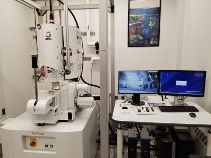
Scanning Electron Microscope

EM  JSM-7900F,  JEOL (Click here for Brochure.)     

SEM_7900F Spec.pdf


Easy Operation Super High Performance FE-SEM:  

  • 0.6 nm @ 15kV,
  • 0.7 nm @ 1kV
SMART:
  •  Auto-functions,
  • Auto-alignment,
  • Every image is a recipe
Detectors: 
  • LED (Lower Electron Detector) - A secondary electron detector system consisting of an in the chamber E-T type detector shall be standard. The user shall have control of the collector cage voltage in a minimum of 5 steps for both SE and BSE imaging.
  • UED (Upper Electron Detector) - A through the lens detector with a user controllable energy filter for collection of topographic (SE) contrast or atomic number (BSE) contrast shall be standard.
  • STEM (Scanning Transmission Detection) – The microscope should be capable of producing STEM images utilizing a STEM converter holder which should be included as standard with the system. The STEM imaging resolution should be 0.8 nm.
  • SRBED (Short Working Distance Retractable Solid State BSE Detector) - The  backscattered electron detector must be a pneumatically retractable (from the GUI) solid state design that does not block SE signal or limit the collection of X-Rays and allows a working distance as short 2.0 mm when inserted. This detector shall produce pure compositional images with a resolution of 0.1Z at Z=29 and be operational at or below 1kV. 
Additional capabilities
  • INCA energy system provides you the capability of semi-quantitative elemental analysis of samples.
  • Cryo-system provides you the capability of imaging hydrated samples.
POWERFUL:
  • Single digit Angstrom resolution at low voltage allowing samples to be viewed in their native state,
  • Detectors with energy filters,
  • Beam deceleration (at any kV, up to 5kV stage bias),
  • STEM-in-SEM standard